- 您现在的位置:买卖IC网 > Sheet目录2000 > IDTSSTE32882HLBBKG (IDT, Integrated Device Technology Inc)IC REGISTERING CLK DRIVER 176BGA
1.35V/1.5V REGISTERING CLOCK DRIVER WITH PARITY TEST AND QUAD CHIP SELECT
26
SSTE32882HLB
7201/14
SSTE32882HLB
1.35V/1.5V REGISTERING CLOCK DRIVER WITH PARITY TEST AND QUAD CHIP SELECT
COMMERCIAL TEMPERATURE
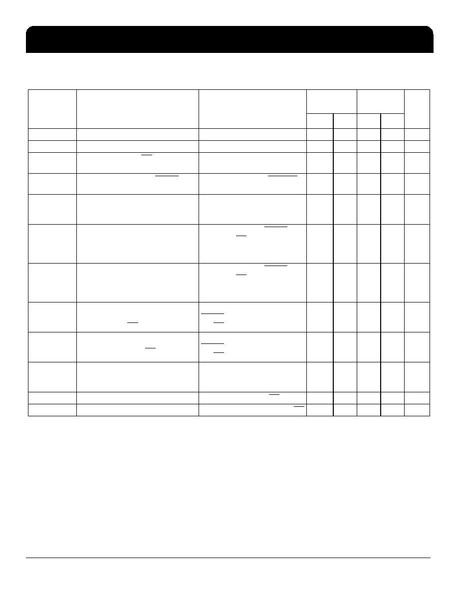
Timing Requirements
Symbol
Parameter
Conditions
DDR3-800/
1066/1333
DDR3-1600
Unit
Min
Max
Min
Max
fCLOCK
Input Clock Frequency
Application Frequency1
1
All specified timing parameters apply.
300
670
300
810
MHz
fTEST
Input Clock Frequency
Test Frequency2
2
Timing parameters specified for frequency band 2 apply.
70
300
70
300
MHz
tCH/tCL
Pulse Duration, CK, CK HIGH or
LOW
0.4
tCK3
3
Clock cycle time.
tACT
Inputs active time before RESET is
taken HIGH4
4
This parameter is not necessarily production tested (see figure below).
DCKE0/1 = LOW and DCS[n:0] =
HIGH
88
tCK3
tMRD
Command word to command word
programming delay
Number of clock cycles between
two command programming
accesses
88
tCK3
tINDIS
Input Buffers disable time after
DCKE[1:0] is LOW
DCKE[1:0] = LOW; RESET =
HIGH; CK/CK = Toggling;
RC9[DBA1] = 1 and RC9[DBA0]
= 0 or 1
1
414
tCK3
tQDIS
Output Buffers Hi-Z after QxCKEn is
driven LOW
DCKE[1:0] = LOW; RESET =
HIGH; CK/CK = Toggling;
RC9[DBA1] = 1 and RC9[DBA0]
= 0 or 1
1.5
tCK3
tCKOFF
Number of tCK required for both
DCKE0 and DCKE1 to remain LOW
before both CK/CK are driven low
DCKE[1:0] = LOW;
RESET = HIGH;
CK/CK = Toggling
55
tCK3
tCKEV
Input buffers (DCKE0 and DCKE1)
disable time after CK/CK = LOW
DCKE[1:0] = LOW;
RESET = HIGH;
CK/CK = LOW
22
tCK3
tFixedoutputs
Static Register Output after DCKE0 or
DCKE1 is HIGH at the input (exit from
Power Saving state)
RC9[DBA1] = 1 and RC9[DBA0]
= 0 or 1
1
314
tCK3
tSU
Setup Time5
5
Setup (tSU) nominal slew rate for a rising signal is defined as the slew rate between the last crossing of VREF(DC) and first
crossing of VIH(AC) min. Setup (tSU) nominal slew rate for a falling signal is defined as the slew rate between the last crossing
of VREF(DC) and the first crossing of VIL(AC) max. If the actual signal is always earlier than the nominal slew rate line between
shaded ‘VREF(DC) to ac region’, use nominal slew rate for derating value. If the actual signal is later than the nominal slew rate
line anywhere between shaded ‘VREF(DC) to ac region’, the slew rate of a tangent line to the actual signal from the ac level to
dc level is used for derating value .
Input valid before CK/CK
100
50
ps
tH
Hold Time6
Input to remain valid after CK/CK
175
125
ps
发布紧急采购,3分钟左右您将得到回复。
相关PDF资料
IDTSSTE32882KA1AKG
IC REGISTERING CLK DRIVER 176BGA
ISD1750SYR
IC VOICE REC/PLAY 50SEC 28-SOIC
ISD5008EYI
IC VOICE REC/PLAY 4-8MIN 28-TSOP
ISL12008IB8Z
IC RTC I2C LO-POWER 8-SOIC
ISL12020MIRZ-T7A
IC RTC/CALENDAR TEMP SNSR 20DFN
ISL12022IBZ-T7A
IC RTC/CALENDAR TEMP SNSR 8SOIC
ISL12022MAIBZ
IC RTC/CALENDAR TEMP SNSR 20SOIC
ISL12022MIBZ-T7A
IC RTC/CALENDAR TEMP SNSR 20SOIC
相关代理商/技术参数
IDTSSTE32882HLBBKG8
制造商:Integrated Device Technology Inc 功能描述:IC REGISTERING CLK DRIVER 176BGA
IDTSSTE32882KA1AKG
功能描述:IC REGISTERING CLK DRIVER 176BGA RoHS:是 类别:集成电路 (IC) >> 时钟/计时 - 专用 系列:- 标准包装:1,500 系列:- 类型:时钟缓冲器/驱动器 PLL:是 主要目的:- 输入:- 输出:- 电路数:- 比率 - 输入:输出:- 差分 - 输入:输出:- 频率 - 最大:- 电源电压:3.3V 工作温度:0°C ~ 70°C 安装类型:表面贴装 封装/外壳:28-SSOP(0.209",5.30mm 宽) 供应商设备封装:28-SSOP 包装:带卷 (TR) 其它名称:93786AFT
IDTSSTE32882KA1AKG8
制造商:Integrated Device Technology Inc 功能描述:IC REGISTERING CLK DRIVER 176BGA
IDTSSTUB32866BHLF
功能描述:IC BUFFER 25BIT CONF REG 96LFBGA RoHS:是 类别:集成电路 (IC) >> 接口 - 专用 系列:- 特色产品:NXP - I2C Interface 标准包装:1 系列:- 应用:2 通道 I²C 多路复用器 接口:I²C,SM 总线 电源电压:2.3 V ~ 5.5 V 封装/外壳:16-TSSOP(0.173",4.40mm 宽) 供应商设备封装:16-TSSOP 包装:剪切带 (CT) 安装类型:表面贴装 产品目录页面:825 (CN2011-ZH PDF) 其它名称:568-1854-1
IDTSSTUB32S869AHLF
功能描述:IC REGISTERED BUFFER 150-TFBGA RoHS:是 类别:集成电路 (IC) >> 接口 - 信号缓冲器,中继器,分配器 系列:- 标准包装:160 系列:- 类型:转发器 Tx/Rx类型:以太网 延迟时间:- 电容 - 输入:- 电源电压:2.37 V ~ 2.63 V 电流 - 电源:60mA 安装类型:表面贴装 封装/外壳:64-TQFP 裸露焊盘 供应商设备封装:64-TQFP-EP(10x10) 包装:托盘 其它名称:Q5134101
IDTSSTUB32S869AHLFT
功能描述:IC REGISTERED BUFFER 150-TFBGA RoHS:是 类别:集成电路 (IC) >> 接口 - 信号缓冲器,中继器,分配器 系列:- 标准包装:160 系列:- 类型:转发器 Tx/Rx类型:以太网 延迟时间:- 电容 - 输入:- 电源电压:2.37 V ~ 2.63 V 电流 - 电源:60mA 安装类型:表面贴装 封装/外壳:64-TQFP 裸露焊盘 供应商设备封装:64-TQFP-EP(10x10) 包装:托盘 其它名称:Q5134101
IDTSSTVF16857AGLF
功能描述:IC DDR REGISTER 48-TSSOP RoHS:是 类别:集成电路 (IC) >> 接口 - 专用 系列:- 标准包装:3,000 系列:- 应用:PDA,便携式音频/视频,智能电话 接口:I²C,2 线串口 电源电压:1.65 V ~ 3.6 V 封装/外壳:24-WQFN 裸露焊盘 供应商设备封装:24-QFN 裸露焊盘(4x4) 包装:带卷 (TR) 安装类型:表面贴装 产品目录页面:1015 (CN2011-ZH PDF) 其它名称:296-25223-2
IDTSTAC9200X3NAEB1X
功能描述:IC AUDIO CODEC 2CH HD 32-QFN RoHS:是 类别:集成电路 (IC) >> 接口 - 编解码器 系列:- 标准包装:2,500 系列:- 类型:立体声音频 数据接口:串行 分辨率(位):18 b ADC / DAC 数量:2 / 2 三角积分调变:是 S/N 比,标准 ADC / DAC (db):81.5 / 88 动态范围,标准 ADC / DAC (db):82 / 87.5 电压 - 电源,模拟:2.6 V ~ 3.3 V 电压 - 电源,数字:1.7 V ~ 3.3 V 工作温度:-40°C ~ 85°C 安装类型:表面贴装 封装/外壳:48-WFQFN 裸露焊盘 供应商设备封装:48-TQFN-EP(7x7) 包装:带卷 (TR)